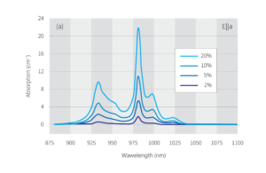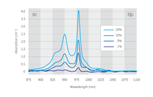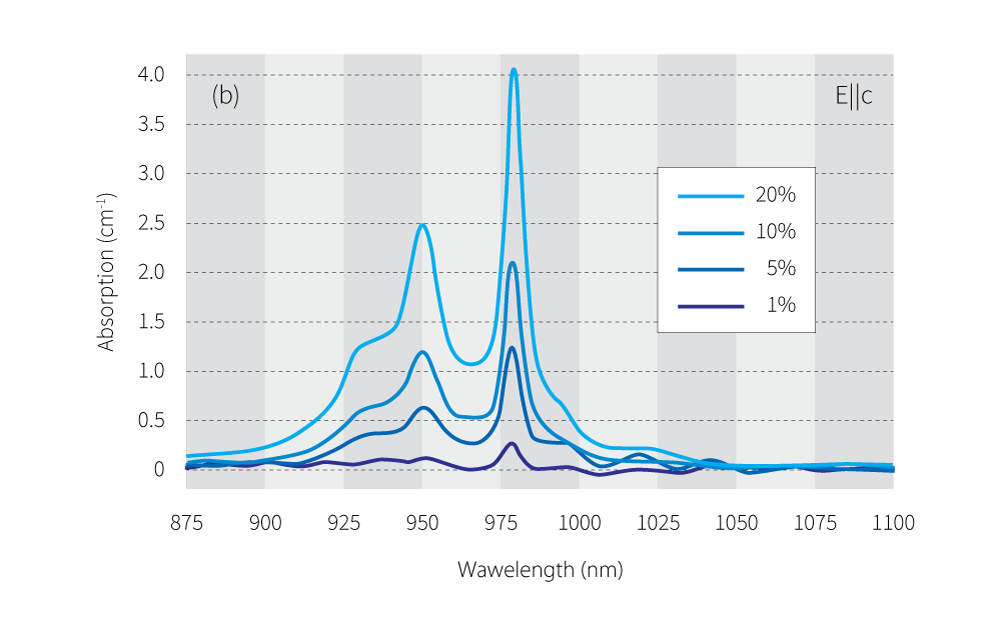
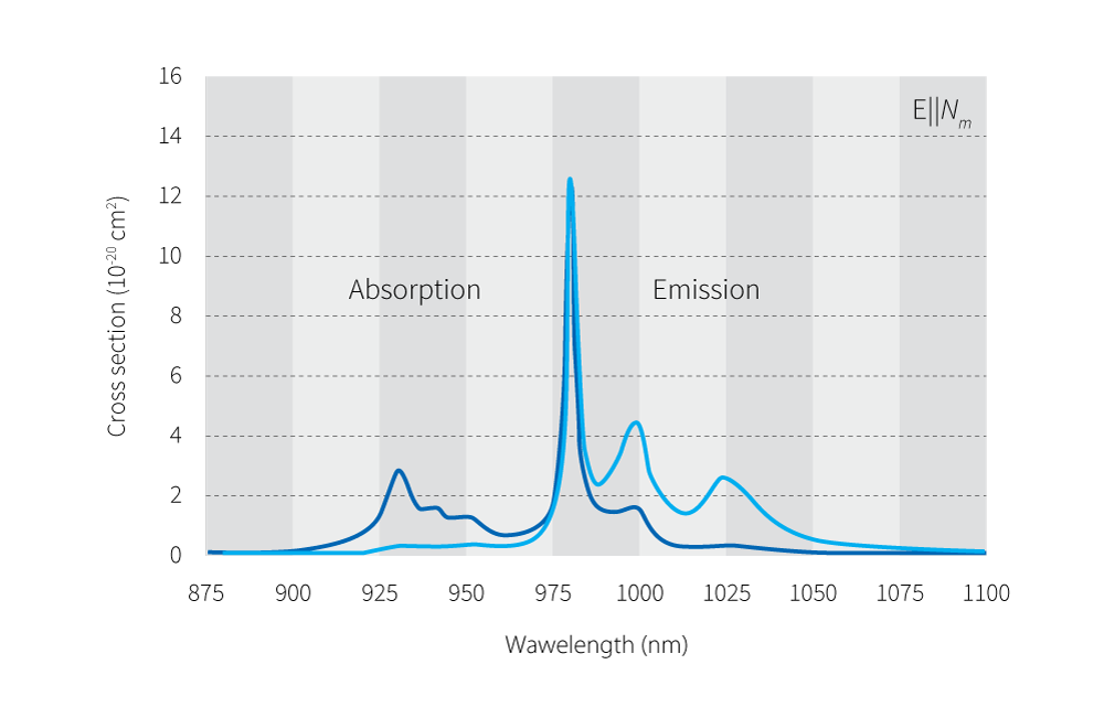
Yb:KGW and Yb:KYW crystals are used as lasing materials to generate ultrashort high-power pulses. The crystals are typically pumped with diode lasers at around 980 nm due to the maximum absorption band around this wavelength. A broad spectral emission band allows tuning of the laser radiation over the 1020 – 1060 nm range.
Yb:KGW and Yb:KYW crystals have already been used for many years, but their performance strongly depends on where the materials were grown. Altechna works with selected material growers and has established a reliable production chain.
To minimize back reflection and improve pump/ lasing performance, broadband antireflective coatings are applied as a rule for all right-angle cut crystals. Coatings are typically made with e-beam and ion-assisted deposition (IAD). However, sputtering technology could also be used if needed.
As a final touch, full metrology of crystals is carried out in our metrology lab.
Contact us for help with your challenge. We have a team of experienced design engineers and metrology capabilities to prototype and transfer your idea into a well-defined production process.